
Fraunhofer FMD - Research Fab Microelectronics Germany
Booth number: H4.E49
www.forschungsfabrik-mikroelektronik.de/en
About us
The Research Fab Microelectronics Germany (Forschungsfabrik Mikroelektronik Deutschland, FMD) is a global innovation driver that, as the largest cross-location R&D cooperation for microelectronics in Europe, offers a unique diversity of expertise and infrastructure. FMD bridges the gap between basic research and customer-specific product development. The FMD is a cooperation of eleven institutes of the Fraunhofer Group for Microelectronics as well as the Leibniz Institutes FBH and IHP.

Address
Anna-Louisa-Karsch-Str. 2
10178 Berlin
Germany
E-mail: armin.wedel@mikroelektronik.fraunhofer.de
Phone: +49 171 5473177
Internet: www.forschungsfabrik-mikroelektronik.de/en
No. 30, M. G. Rd.
560 001 Bangalore
India
E-mail: anandi.iyer@fraunhofer.in
Phone: +91 80 409650089
Internet: www.fraunhofer.in
Contact person:
Dr. Armin Wedel
Business Development International
E-mail: armin.wedel@mikroelektronik.fraunhofer.de
Phone: +49 171 5473177
Dr. Christoph Kroh
Manager Business Development
E-mail: christoph.kroh@mikroelektronik.fraunhofer.de
Phone: +49 171 3553729
Dr. Stephan Guttowski
Managing Director
E-mail: stephan.guttowski@mikroelektronik.fraunhofer.de
Phone: +49 172 8166781
Products & Services
APECS – Advanced Packaging and Heterogeneous Integration for Europe’s Next Generation Semiconductor Technologies
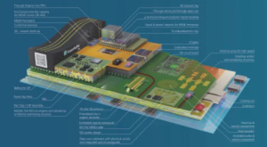
APECS (Advanced Packaging and Heterogeneous Integration for Electronic Components and Systems) is a European pilot line dedicated to accelerating innovation in semiconductor technologies through advanced packaging and heterogeneous integration. As part of the European Chips Act initiative, APECS provides companies, research organizations and start-ups with access to state-of-the-art technologies, expertise and services to develop, test and scale next-generation electronic systems. The pilot line combines leading European research capabilities from Fraunhofer and Leibniz institutes, offering solutions in areas such as high-performance packaging, multi-material integration, sensor technologies and advanced semiconductor architectures. APECS supports industry-driven innovation by enabling collaboration across the semiconductor ecosystem – from research and development to industrial applications. Companies and start-ups can benefit from open access opportunities, technology expertise and networking with key players across Europe. We are looking for new partners, innovative companies and start-ups interested in exploring collaboration opportunities, technology development and solutions for future semiconductor applications.