
LASER World of PHOTONICS INDIA 2026 + productronica India 2026Products & Services Openair-Plasma®: Semiconductor
Openair-Plasma®: Semiconductor
Exhibitor
Plasmatreat Asia Pacific Pte Ltd
Openair-Plasma® in Semiconductor Packaging plasma cleans and activates surfaces inline, quickly and in a controlled manner. In the semiconductor industry in particular, this enables highly particle-free process control, which reduces waste and increases quality. In addition to perfect adhesion and optimal wettability, service life and product stability also benefit: interface failures such as delamination (IDM) or internal cracking (CCM) can be significantly minimized through targeted plasma pretreatment.
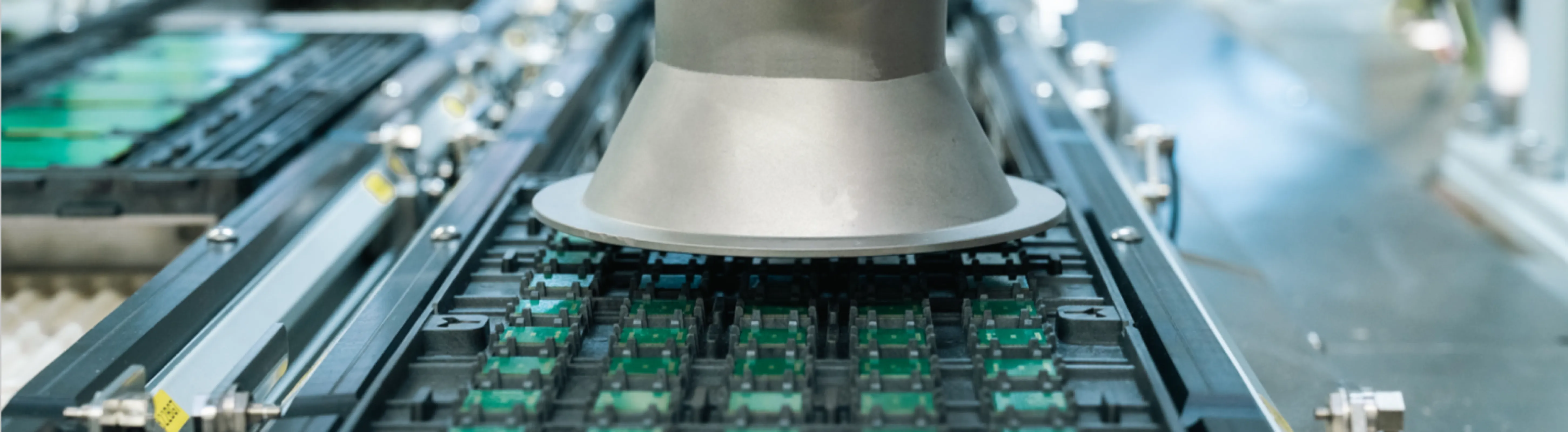
Openair-Plasma® in Semiconductor Packaging